
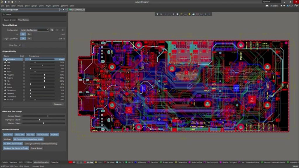
With over 47 years of manufacturing experience, Burton EMS is dedicated to providing expert insights into printed circuit board schematics, performance, manufacturability, and cost-effectiveness. In the rapidly evolving world of electronics, the design and development of printed circuit board assemblies (PCBAs) play a crucial role in ensuring the performance and reliability of modern devices. Our commitment to quality and innovation ensures that your electronic designs are not only functional but also optimized for production. At Burton EMS, we specialize in various PCBA layout services. We use the industry standard Altium Designer software and verify using VAYO Intelligent DFA/DFM tools to guarantee precision and reliability.
Stack-up/Build-up Development
- Design and development of internal PCB structures.
- Optimization of layer configurations for enhanced performance.
- Ensuring thermal management and signal integrity.
Transmission Line Configuration
- Conductivity and impedance profile calculations to ensure optimal performance.
- Custom transmission line designs tailored to specific application requirements.
- Simulation and testing to validate electrical performance.

Multi-Layer PCB Design
- Expertise in building high-density circuits with 12+ layers.
- Incorporating multiple conductive signal layers and power planes.
- Ensuring reliability through rigorous testing and validation.
High-Speed PCB Design
- Development of high-speed interfaces, including multi-GHz SerDes lines.
- Expertise in LVDS, DDR2/3/4 memory, USB, PCIe, and SATA design.
- Signal integrity analysis and mitigation of electromagnetic interference (EMI).
Radio-Frequency (RF) PCB Design
- Specialized device layouts for wireless data exchange functionalities such as Wi-Fi, Bluetooth, GSM, and GPS.
- Design for low noise and high-frequency stability.
- Integration of RF components with minimal signal loss.

High-Density Interconnect PCBs (HDI)
- Creation of PCBs with finer lines and spaces.
- Utilizing advanced technologies like blind and buried vias, uVIA, and via-in-pad for fine-pitch ICs.
- Ensuring high performance and reliability in compact designs.
Flex and Rigid-Flex PCB Design
- Design of complex PCB structures with flexible sections.
- Integration of rigid parts with flexible connectors.
- Durability testing for dynamic and static applications.
Design for Supply Chain
- Component life-cycle and risk analysis to ensure availability.
- B.O.M. (Bill of Materials) scrub for accuracy and efficiency.
- Single source and lead time review to prevent delays.
- Obsolescence management to avoid production disruptions.
- Recommendation of cross-references and substitutes for critical components.
Design for Manufacturing (DFM)
- Core expertise in eliminating potential manufacturing issues, backed by 46 years of manufacturing excellence.
- Utilization of advanced DFM software for adherence to IPC guidelines and beyond.
- Ensuring repeatability and reliability in production.
- 3D simulation of assembled boards to visualize and troubleshoot designs before production.
- Continuous improvement processes to enhance manufacturability and reduce costs.
Creating sophisticated PCBA designs demands a meticulous approach to guarantee optimal performance, reliability, and manufacturability. Every phase, from initial design and layer configuration to the final stages of testing and validation, is crucial for achieving the desired results. By utilizing advanced technologies and following best practices in supply chain and manufacturing design, engineers can develop PCBAs that meet the rigorous requirements of modern electronic applications. For any questions, concerns, or project inquiries, please contact us at [email protected].
